ASIC IP and Design Services Company Krish Semiconductors was established by a group of experienced experts with a focus on providing top-notch services for clients’ difficult designs. Krish Semiconductors is afast growing company with over 100 years of combined experience in the design and production of semiconductor chips.
EXPERIENCE WITH FULL CHIP/BLOCK DEVELOPMENT WITH TIME CLOSURE FOR TASK SUCH AS SYNTHESIS, FLOOR PLAN, PLACEMENT, CTS, SIGNAL INTEGRITY, IR DRAW, EM, LOW POWER CHECKS AND SIGNOFF CHECKS. AN EXTENSIVE UNDERSTANDING OF PHYSICAL VERIFICATION, SUCH AS DRC, LVS, ANTENNA, AND DENSITY IN RECENT NODES, SUCH AS 14NM, 10NM. DFT TECHNIQUES SUCH AS SCAN, BIST, ATPG, AND BOUNDARY SCAN WORKING KNOWLEDGE
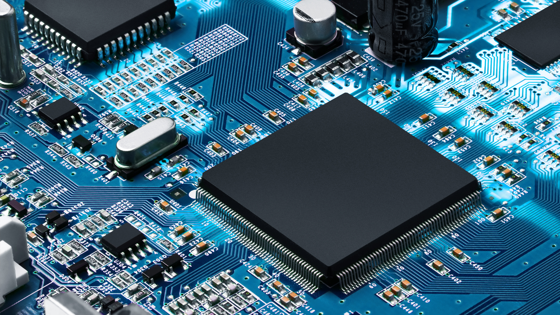
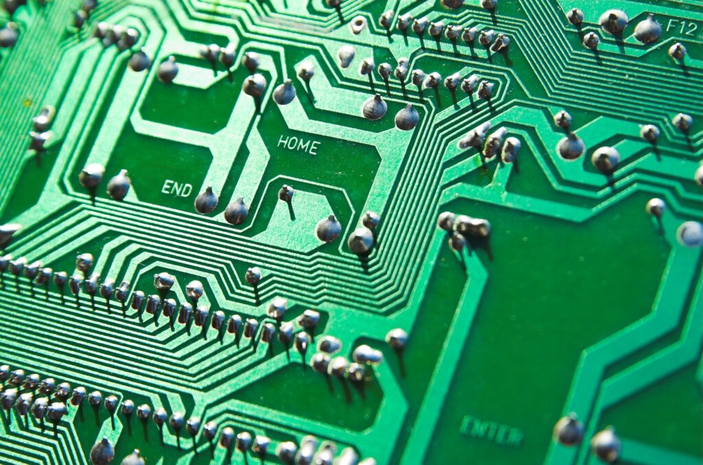
PHYSICAL DESIGN
The following points of competence are included in Krish Semiconductors’s Physical Design Services offerings.
Learn More
DFT IMPLEMENTATION
The DFT Service offerings of Krish Semiconductors include competence in the following sectors.
Learn More
STAFF AUGMENTATION
By offerings your business with the appropriate staff augmentation services-implement cost-effective initiatives.
Learn More
Contact us
Give us a call or drop by anytime, we endeavour to answer all enquires within 24 hours on business days. We will be happy to answer your questions.